
- * 프린트는 Chrome에 최적화 되어있습니다. print
반도체 소재·부품 대학원 / Graduate School of Semiconductor Materia

정건욱 Kunook Chung
반도체 소재·부품 대학원 / Graduate School of Semiconductor Materia
 +82-52-217-2039
 kunookc@unist.ac.kr
 Bldg. 108 Rm. 601-10(Office)
Curriculum Vitae
• Assistant Professor in Department of Physics, UNIST, Korea. (2019 - present)
• Postdoctoral in Department of Electrical Engineering and Computer Science, University of Michigan, US. (2015 - 2019)
• Postdoctoral in Department of Physics and Astronomy, Seoul National University, Korea. (2015)
Education
Academic Credential
Ph.D. in Physics, Seoul National University, Korea. (2015)
We are interested in utilizing unique physical properties of various low dimensional (D) nanomaterials, such as 2D van der Walls layered materials, 1D nanorods (and nanopillars), and 0D quantum dots, as key building blocks for fabricating high performance and new functional semiconductor optoelectronic devices. Details of the current research interests are:
• Metal-organic chemical vapor deposition and chemical vapor deposition of high quality semiconductor microstructures and nanostructures, 2D van der Walls layered materials, and their hybrids.
• Fabrications of high performance optoelectronic devices, such as light emitting diodes, solar cells, and sensors.
• Strain engineering of semiconductor heterostructures and quantumstructures using nanofabrication and/or heteroepitaxial growth.
• Diverse device applications including transferable and wearable devices, full-color inorganic microdisplays, augmented reality, quantum computing and communications, neural probes, and so on.
Major research field
Desired field of research
Research Publications
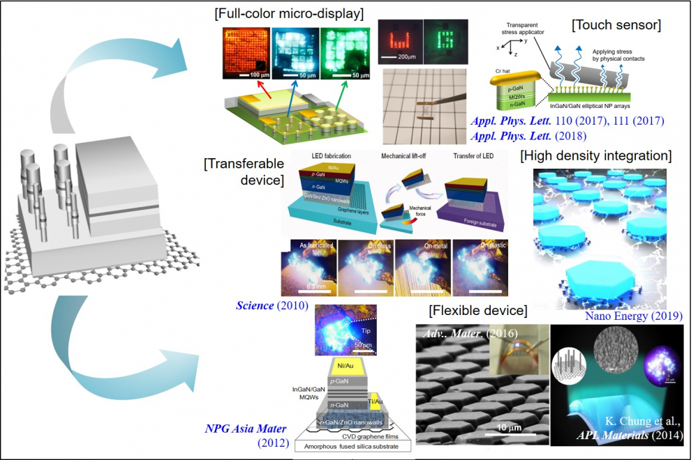
MORE- K. Chung, K. Lee, Y. Tchoe, H. Oh, J. Park, J. K. Hyun, G.-C. Yi, GaN microstructure light-emitting diodes directly fabricated on tungsten-metal electrodes using a micro-patterned graphene interlayer, Nano Energy 60, 82 (2019).
- K. Chung, J. Sui, B. Demory, C.-H. Teng, P.-C. Ku, Monolithic integration of individually addressable light- emitting diode color pixels, Appl. Phys. Lett. 110, 111103 (2017).
-K. Chung, C.-H. Lee, and G.-C. Yi, Transferrable GaN layers grown on ZnO-coated graphene layers for optoelectronic devices, Science 330, 655 (2010).
Patents
- Color mixing monolithically integrated light-emitting diode pixels, P.-C. Ku, K. Chung, B. Demory, US 10708995, 2020.7.7.
- Optical device and method for manufacturing same, G.-C. Yi, K. Chung, US 9444006, 2016.9.13.