
- * 프린트는 Chrome에 최적화 되어있습니다. print
반도체 소재·부품 대학원 / Graduate School of Semiconductor Materia

김정환 Junghwan KIM
반도체 소재·부품 대학원 / Graduate School of Semiconductor Materia
 +82-52-217-3214
 j.kim@unist.ac.kr
 https://sites.google.com/view/futurematerials/home?pli=1
 Bldg. 102 Rm. 401-10
Curriculum Vitae
· 2023.01~, Assistant Professor, Graduate School of Semiconductor Materials and Devices Engineering, UNIST
· 2023.01~, Specially Appointed Associate Professor, MDX research center for Element Strategy, Tokyo Institute of Technology
· 2021.10~, PRESTO Researcher, JST
· 2021.12~, Adjunct Professor, Department of Chemical Engineering, POSTECH
· 2019.04~2021.03, Visiting Researcher, National Institute for Materials Science (NIMS)
Academic Credential
· 2014.04~2016.03, Innovative and Engineered Materials, Tokyo Institute of Technology (Doctor of Engineering)
· 2012.10~2014.03, Innovative and Engineered Materials, Tokyo Institute of Technology (Master of Engineering)
· 2005.03~2012.08, Electrical and Computer Engineering, Ajou University (Bachelor of Engineering)
Awards/Honors/Memberships
· 2022.04 Minister of Education, Culture, Sports, Science and Technology, The Young Scientists' Award
· 2020. 06 Tokyo Tech Challenging Research Award
· 2017.02 Inoue Research Award for Young Scientists
· 2016.09 Young Scientist Award, The Japan Society of Applied Physics
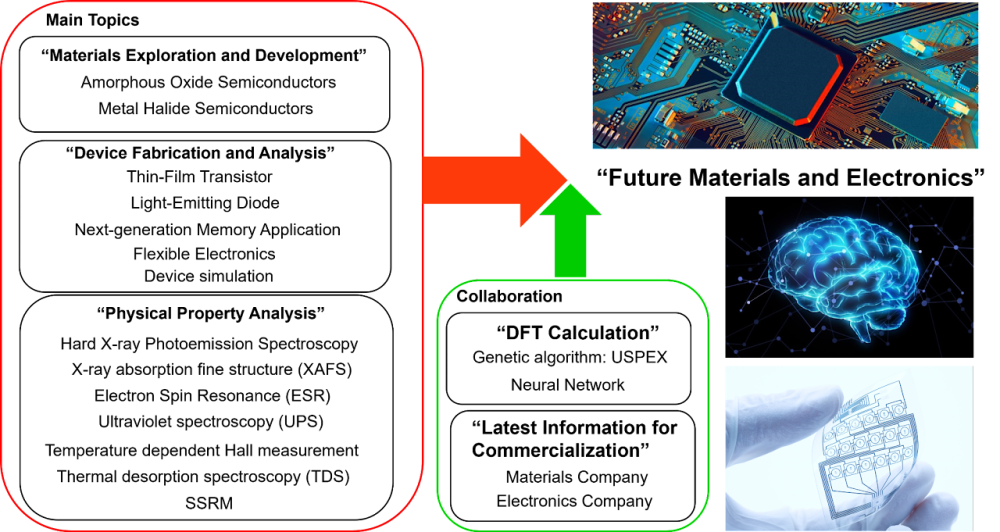
Over the past several decades, Si has been the representative electronic material in the field of semiconductor electronics. Nevertheless, our society has steadily become interested in the following topics of “energy harvesting”, “eco-friendly”, “low-power consumption”, etc. In this respect, quite many new materials have been proposed to date. Recently, “Materials Informatics” has accelerated the exploration of new materials. However, this background makes it difficult more and more to judge which material is better among a lot of candidates. Indeed, the most critical drawback is the difficulty in understanding of all the new materials in terms of “material science” as different materials possess different physical properties such as charge transport or doping mechanism and defects control; process also differs a lot according to materials. In this respect, “physical property analysis” plays a crucial role in understanding fundamentals. I have experienced a variety of skills of “physical property analysis”. Based on the “physical property analysis” skills, I have designed various new materials and developed the relevant electronic devices.
***Development of Next-Generation Electronics utilizing New Concepts and New Materials***
1. High-density Integration of Metal Oxide Electronics
High-density integration is essential in the field of electronics industry. However, for metal oxide electronics such as oxide thin-film transistors, the channel length is still several micrometers. Trade-off between contact resistance and hydrogen impurity induced channel shortening has been known to be responsible for the current drawback. In future research, I will clarify the role of hydrogen impurity in oxide semiconductors and design new oxide semiconductor that is robust to hydrogen impurities, which will be the route to the high-density integration of oxide electronics. It also realizes new electronics combining conventional Si electronics and oxide electronics.
2. Neuromorphic Devices
Artificial intelligence (AI) technologies attract much attention; machine learning techniques based on neural network algorithm have already been used to explore new materials. Accordingly, neuromorphic electronics are recently highly demanded. ReRAM and memristors have emerged as promising candidates for neuromorphic electronics; both exhibits resistive switching behavior. Mostly, metal oxides have been used for ReRAM in which oxygen vacancy defect (VO) plays a crucial role of resistive switching. However, it is still not clear whether VO based ReRAM is the best in terms of switching speed. Recently, I have already confirmed the validity of H- ion conduction in resistive switching. In future research, I will explore more various candidate materials for Neuromorphic Devices.
Major research field
반도체 소재, 메모리, 트랜지스터, 발광소자, 물성 분석
Desired field of research
신소재공학, 전자공학, 화학, 물리 / Materials Science, Electrical Engineering, Chemistry, Physics
Research Keywords and Topics
비정질 산화물 반도체, 페로브스카이트 반도체, 트랜지스터, 발광소자, 재료 물성 및 결함 분석
Amorphous Oxide Semiconductors, Perovskite Semiconductors, Field-effect Transistors, Light-emitting diodes, Materials & Defect Characterization
Research Publications
· Nature Electronics, Mobility-Stability Trade-off in Oxide TFTs, Y. Shiah, K. Sim, Y. Shi, K. Abe, S. Ueda, M. Sasase, J. Kim*, H. Hosono*, 2021 .11
· Advanced Materials, Lead-free Highly Efficient Blue-emitting Cs3Cu2I5 with 0D Electronic Structure, 29. T. Jun, K. Sim, S. Iimura, H. Kamioka, M. Sasase, J. Kim*, H. Hosono*, 2018. 9
· Advanced Materials, Material Design of p‐Type Transparent Amorphous Semiconductor, Cu–Sn–I, 30. T. Jun, J. Kim*, M. Sasase, H. Hosono*, 2018.1
국가과학기술표준분류
- ED. 전기/전자
- ED04. 반도체소자·시스템
- ED0405. 반도체 재료
국가기술지도분류
- 정보-지식-지능화 사회 구현
- 010400. 반도체/나노 신소자 기술
녹색기술분류
- 고효율화기술
6T분류
- IT 분야
- 핵심부품
- 010114. 고밀도 정보저장장치 기술