
- * 프린트는 Chrome에 최적화 되어있습니다. print
Graduate School of Semiconductor Materia / 반도체 소재·부품 대학원
Byungjo Kim 김병조
Graduate School of Semiconductor Materia / 반도체 소재·부품 대학원
 +82-52-217-3215
 bold.kim@unist.ac.kr
 https://sites.google.com/view/bkimlab
 Bldg. 102 Rm. 401-9
Curriculum Vitae
· 2024~present: Assistant Professor, UNIST
· 2019~2023: Staff Engineer, Mechatronics Research, Samsung Electronics Co. Ltd.
Academic Credential
· 2019: Ph.D., Mechanical Engineering, Seoul National University
· 2011: B.S., Mechanical Engineering, POSTECH
Awards/Honors/Memberships
· 2022: Samsung Best Paper Award Bronze (Samsung Electronics Co., Ltd)
· 2019: Excellent Doctoral Thesis Award (KSME)
· 2017~2019: Ph.D. Sponsorship Program (Samsung Electronics Co., Ltd)
· 2016: KSME-SEMES Open Innovation Challenge Bronze (KSME)
· 2004~2011: National Scholarship for Science and Engineering (KOSAF)
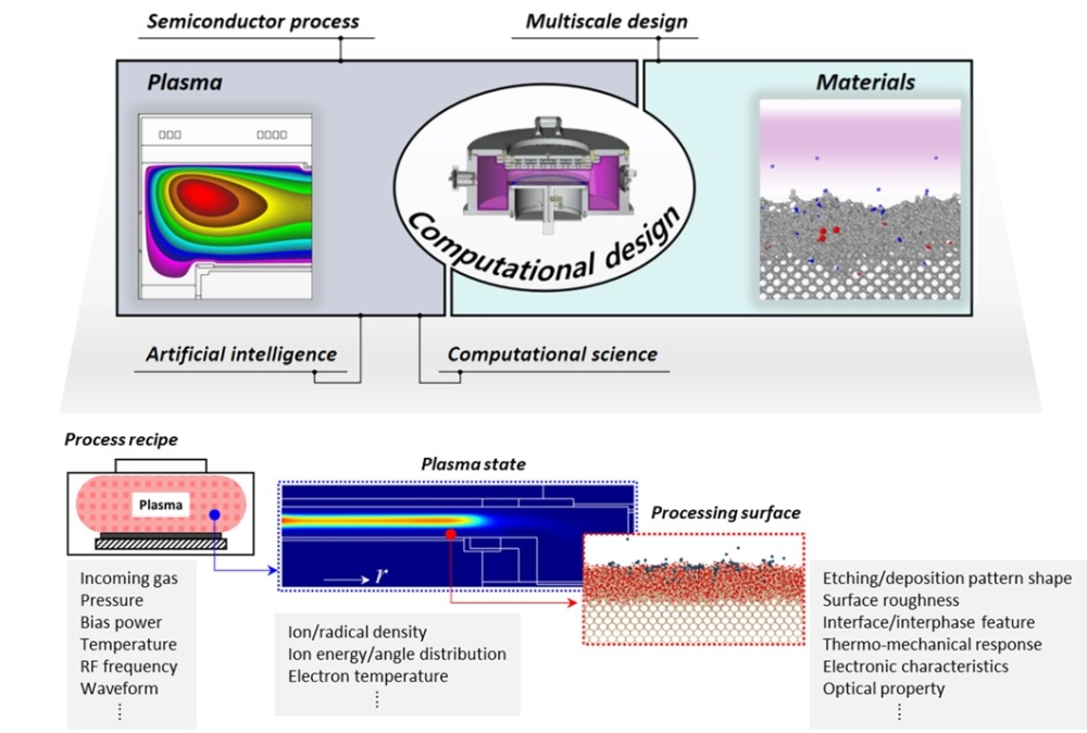
The Virtual Materials and Processes Design Laboratory (VDLab) endeavors to develop highly sophisticated methodologies for an essential understanding and innovative design of materials and processes across a broad spectrum, encompassing multiscale phenomena from quantum to continuum mechanics. By leveraging novel scale-bridging techniques, the laboratory addresses complex challenges in plasma-material interactions, which are pivotal for semiconductor processing. The VDLab is dedicated to optimizing material and process variables, employing multiphysics computational simulations to enhance the performance and yield of semiconductor manufacturing.
Major research field
Multiscale simulation, Semiconductor materials and processes, Plasma-materials interaction, Functional soft materials
Desired field of research
Advanced scale-bridging, High-power computing for simulation, Machine learning in materials science, Sustainable semiconductor processing, New material discovery for semiconductor applications
Research Keywords and Topics
Multiscale simulation, Semiconductor materials and processes, Plasma-materials interaction, Machine learning in materials science, Molecular dynamics, Nanocomposites, Density functional theory
Research Publications
· Journal of Physics D: Applied Physics / Deep neural network-based reduced-order modeling of ion–surface interactions combined with molecular dynamics simulation / Byungjo Kim et al., / 2023-09
· Journal of Physics D: Applied Physics / Computational approach for plasma process optimization combined with deep learning model / Byungjo Kim et al., / 2023-08
· Surfaces and Interfaces / Combined molecular dynamics simulations and reaction kinetics study on wettability of Trimethylsilyl functionalized silicon surfaces / Byungjo Kim et al., / 2022-12
· Applied Surface Science / Atomistic insights on hydrogen plasma treatment for stabilizing High-k/Si interface / Byungjo Kim et al., / 2022-08
Patents
· Upper electrode and substrate processing apparatus including the same / Byungjo Kim et al., / Published No.(US):11,545,344B2 / 2023-01
· Bonding head, die bonding apparatus including the same and method of manufacturing semiconductor package using the same / Byungjo Kim et al., Published No.(US):11,626,381B2 / 2023-04
국가과학기술표준분류
- EA. 기계
- EA02. 생산기반기술
- EA0207. 예측/시뮬레이션기술
국가기술지도분류
- 정보-지식-지능화 사회 구현
- 010400. 반도체/나노 신소자 기술
녹색기술분류
- 무공해산업기술
- 가상현실
- 511. 가상현실기술
6T분류
- IT 분야
- 핵심부품
- 010114. 고밀도 정보저장장치 기술