
- * 프린트는 Chrome에 최적화 되어있습니다. print
기계공학과 / Mechanical Engineering

노윤수 Yoonsoo Rho
기계공학과 / Mechanical Engineering
 +82-52-217-2442
 yrho@unist.ac.kr
 https://sites.google.com/view/yrho
 Bldg. 112 Rm. 701-3
Curriculum Vitae
· 2024~Present: Assistant Professor, UNIST, Korea
· 2022~2024: Staff Scientist, Lawrence Livermore National Laboratory (LLNL), CA, USA
· 2021~2022: Post-doctoral Research Fellow, University of California, Berkeley, CA, USA
· 2017~2023: Research Engineer, Laser Prismatics, CA, USA
· 2012~2015: Researcher, Korea Institute of Industrial Technology (KITECH), Korea
Academic Credential
· 2021: Ph.D. in Mechanical Engineering, University of California, Berkeley
· 2012: M.S. in Mechanical Engineering, Korea Advanced Institute of Sci &Tech (KAIST)
· 2010: B.S. in Mechanical Engineering, Korea Advanced Institute of Sci &Tech (KAIST)
Awards/Honors/Memberships
· 2020: Frank and Margaret Lucas Scholarship Fund
· 2019: Best Presentation Award, Conference on Laser Ablation
· 2019: Lloyd Burr Memorial Endowment Fund
· 2012: Scholarship for Global Internship Program, National Research Foundation of Korea
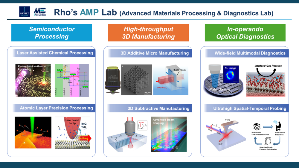
첨단 소재 가공 및 계측의 발전은 고성능 디바이스의 지속적인 성능 향상과 소형화에 중요한 역할을 해왔습니다. 저희 연구실은 레이저-물질 상호작용 기반의 첨단 소재 가공 및 진단 기법을 개발합니다. 이를 통해 다양한 신소재 (반도체, 저차원, 양자점 물질) 및 최신 과학적 개념을 유용한 디바이스 개발에 적용합니다. 구체적으로 저희 연구실은 i) 원자층 정밀 식각, 도핑, 합성, ii) 초고속, 초고해상도 3D 적층 제조, iii) 웨이퍼 규모의 다중 모드 진단 및 데이터 기반 소자 성능 예측, 공정 최적화와 관련된 연구를 수행합니다. 이러한 혁신을 통해, IoT, 에너지, 헬스케어, 국방분야에 적용가능한 첨단 소재/기술 기반 고성능 디바이스를 개발하며, 궁극적으로 연구실 단위에 머물고 있는 나노테크놀로지를 산업으로 이전하는데 기여하고자 합니다.
Advancements in materials fabrication and metrology have played a crucial role in the ongoing development and miniaturization of high-performance electronic and photonic devices. My research program focus on applying fundamental discovery of science and technology to the new manufacturing process and related device applications, including 1) an atomic layer precision etching, doping, synthesis, ii) a high-throughput, high-resolution 3D additive manufacturing, and iii) wafer-scale multimodal characterization and data-driven prediction of device failure and process optimization. These innovations will bridge the gap between fundamental discoveries in nanoscience and technology and practical, commercially viable devices with unprecedented performances, and ultimately facilitate “nanotechnology from lab to industry”.
Major research field
레이저 공정, 레이저 측정, 광역 광학 진단, 초고속 나노스케일 측정, 반도체 공정, 3D 적층 제조, 광전자 소자 제조 및 측정
Desired field of research
초고속 3D 적층 제조, 반도체 패키징 공정, 레이저 공정의 디지털 트윈 기술, 양자 센서 응용기술
Research Keywords and Topics
레이저 가공, 레이저 측정, 반도체 가공, 전자 소자, 광전자 소자, 마이크로/나노 공학, 광학 진단
Laser Processing, Semiconductor Processing, Electronic, Optoelectronic Device, Micro/Nano Engineering, Optical Diagnostics
Research Publications
· Nature Electronics, “A laser-assisted chlorination process for reversible writing of doping patterns in graphene,” Y. Rho‡, K. Lee‡, L. Wang, Y. Chen, C. Ko, P. Ci, J. Pei, A. Zettl, J. Wu and C. P. Grigoropoulos, Aug 2022
· Nano Letters, “Plasmonic nonlinear energy transfer enhanced second harmonic generation nanoscopy,” Y. Rho‡, S. J. Yoo‡, D. Durham, D. J. Kang, A. Minor, and C. P. Grigoropoulos, Feb 2023
· Nano Letters, “Ultrafast Optical Nanoscopy of Carrier Dynamics in Silicon Nanowires,” J. Li‡, R. Yang‡, Y. Rho*, P. Ci, M. Eliceiri, J. Wu, and C. P. Grigoropoulos*, Jan 2023
· Optics Letters, “Wide-field probing of silica laser-induced damage precursors by photoluminescence photochemical quenching,” Y. Rho, C. F. Miller, R. E. Yancey, T. A. Laurence, C. W. Carr, J. H. Yoo, July 2023
Patents
· Y. Rho et al., “Dielectric layer, device for storing energy with the dielectric layer and method for manufacturing thereof,” 2018, Korean Patent No. 1019120170000
· Y. Rho et al., “Method for forming conductive layer patterns by inkjet-printing,” 2017, Korean Patent No. 1018087410000
· Y. Rho et al., “Electrohydro dynamic spray nozzle module,” 2015, Korean Patent No. 1015619940000
국가과학기술표준분류
- EA. 기계
- EA06. 나노·마이크로기계시스템
- EA0604. 초소형 가공/조립/측정기술
국가기술지도분류
- 정보-지식-지능화 사회 구현
- 010400. 반도체/나노 신소자 기술
녹색기술분류
- 고효율화기술
- 친환경 제조공정 및 소재효율성 향상
- 352. 제조공정/소재 효율성 향상 기타 기술
6T분류
- NT 분야
- 나노기반/공정
- 030416. 나노패터팅 공정기술