

Faculty Research Profile

Heechun Park


학력
· 2018: Ph.D. in EECS, Seoul National University
· 2011: B.S. in EE, Seoul National University
주요 경력
· 2024~present: Assistant Professor, UNIST
· 2022~2024: Assistant Professor, Kookmin University
· 2021~2022: BK Assistant Professor, Seoul National University
· 2020~2021: Senior Researcher, Seoul National University
· 2018~2020: Postdoc. Fellow, GeorgiaTech
수상/학회/외부활동
TPC member, Design Automation Conference (DAC), 2025
TPC member, Asia and South Pacific Design Automation Conference (ASP-DAC), 2025, 2026
OC member, Asia and South Pacific Design Automation Conference (ASP-DAC), 2024, 2025
Division Chair (N. VLSI CAD), Korean Conference on Semiconductors (KCS), 2025, 2026
Program Vice Chair, IEIE SoC Conference, 2023
반도체설계자동화연구실
Semiconductor Design Automation Lab (SeDA Lab)
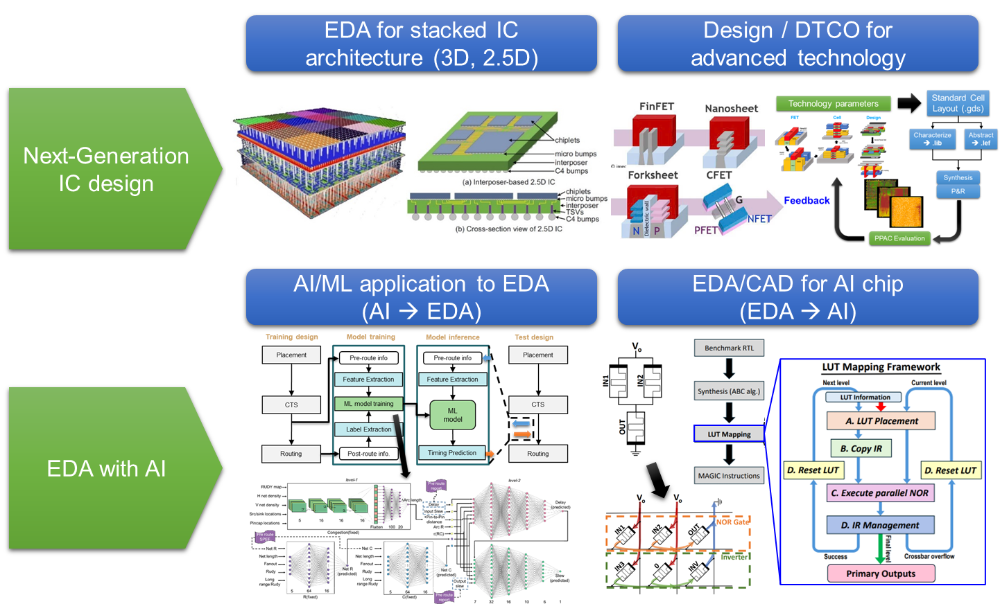
반도체설계자동화 연구실은 시스템온칩 및 고밀도 집적회로의 설계를 위한 컴퓨터이용설계(CAD) 솔루션을 연구합니다. 다양한 디지털 IP 및 칩에 대해 전력, 성능, 면적, 설계 시간 등의 관점에서 가장 효율적으로 설계할 수 있는 전자설계자동화 (EDA) 프레임워크를 구축하는 것을 목표로 연구를 진행하고 있습니다. 현재 (1) 차세대 집적회로 구조(3D, 2.5D, 선단 공정 등)에 대한 EDA 및 (2) 인공지능과의 융합 연구(EDA를 위한 인공지능, 인공지능을 위한 EDA)로 분야를 확장하고 있습니다.
SeDA lab. focuses on researching and developing computer-aided design (CAD) solutions for SoC & VLSI. Our goal is to build electronic design automation (EDA) frameworks for cutting-edge digital IPs/chips with short time-to-market (TTM) and optimized power, performance, area, and cost (PPAC). We are extending our research coverage in the direction of (1) next-generation integrated chip (IC) structures, such as 3D ICs, chiplet-based 2.5D ICs, and under advanced technology nodes; and (2) EDA with AI in both directions: AI for EDA (AI/ML application to EDA) and EDA for AI (EDA framework for AI chip design)
SeDA lab. focuses on researching and developing computer-aided design (CAD) solutions for SoC & VLSI. Our goal is to build electronic design automation (EDA) frameworks for cutting-edge digital IPs/chips with short time-to-market (TTM) and optimized power, performance, area, and cost (PPAC). We are extending our research coverage in the direction of (1) next-generation integrated chip (IC) structures, such as 3D ICs, chiplet-based 2.5D ICs, and under advanced technology nodes; and (2) EDA with AI in both directions: AI for EDA (AI/ML application to EDA) and EDA for AI (EDA framework for AI chip design)
연구분야
Electronic Design Automation & Computer-Aided Design, AI/ML application to EDA
Electronic Design Automation & Computer-Aided Design, AI/ML application to EDA
연구주제
Electronic design automation (EDA), Computer-aided design (CAD), 3D IC, 2.5D IC, Design-technology co-optimization (DTCO), AI-EDA, MLCAD, AI chip design
Electronic design automation (EDA), Computer-aided design (CAD), 3D IC, 2.5D IC, Design-technology co-optimization (DTCO), AI-EDA, MLCAD, AI chip design
국가연구개발사업 기술 분류체계
국가과학기술표준분류
ED. 전기/전자 > ED04. 반도체소자·시스템 > ED0407. 설계 Tool
논문
· Gyumin Kim and Heechun Park, "A Unified Design Flow for Homogeneous and Heterogeneous 3D Integration with Fine-Pitch Hybrid Bonding", IEEE/ACM International Conference on Computer-Aided Design (ICCAD), 2025
· Junghyun Yoon and Heechun Park, "Mitigating Routability Problems in Complementary-FET-based VLSI Designs", IEEE/ACM Design Automation Conference (DAC), 2025
· Dhoui Lim and Heechun Park, "Timing-Driven Detailed Placement with Unsupervised Graph Learning", IEEE/ACM Design, Automation and Test in Europe Conference (DATE), 2025
특허
· "심층 신경망을 위한 뉴로모픽 컴퓨팅 구조의 최적화 시스템", 한국, 등록번호 10-2353816, 2022년 1월 17일
· "신호 전달을 위한 주 경로 및 우회 경로를 갖는 집적 회로 및 그것을 포함하는 집적 회로 패키지", 한국, 등록번호 10-2125340, 2020년 6월 16일